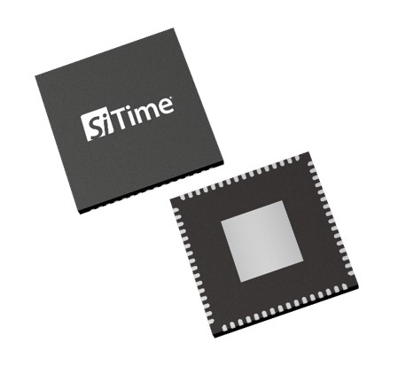
Low Jitter, 11-output MEMS Clock Generator
The Cascade™ SiT95143 is a single-chip MEMS clock generator optimized for the highest level of clock tree integration. This clock-system-on-a-chip (ClkSoC) consolidates multiple clock ICs and oscillators into a single device. Its low noise quad-PLL architecture and programmable output drivers provide up to 10 differential or 20 LVCMOS low-jitter clock outputs. It supports 4 additional clock inputs with Frac-N dividers, enabling virtually any input-to-output frequency translation configurations from 8 kHz to 2.1 GHz.
该时钟发生器集成了Sentime的第三代MEMS谐振器。该集成MEMS方法消除了对晶体参考和石英相关问题的传统时钟依赖性,并提高了系统鲁棒性:
- Always accurate clock synthesis by eliminating crystal capacitive mismatch
- Always reliable startup even at cold temperature and in other harsh environmental conditions
- No jitter degradation because of noise coupling onto a crystal interface
- 无活动倾斜/频率跳跃与Quartz固有
- 10倍的抗振动和弯曲
The SiT95143 is supported by TimeMaster™ software that simplifies clock tree design. The device can also be shipped with a user-specified, factory pre-programmed default startup configuration. The device configuration can be re-programmed twice using two banks of one-time-programmable (OTP) memory during manufacturing or configured in-system via I2C/SPI for additional BOM flexibility. The SiT95143 is also supported with the SiT6503EB evaluation board.
View related products:10个产出
| Number of Inputs | 4 |
| Number of Outputs | 11 |
| Input Frequency Range | 8 kHz至2.1 GHz(差速器),8 kHz至250 MHz(LVCMOS) |
| 输出频率范围 | 8 kHz至2.1 GHz(差速器),8 kHz至250 MHz(LVCMOS),1 PPS(仅一次输出) |
| Output Type | LVPECL, CML, HCSL, LVDS, LVCMOS |
| PLL /时钟域的数量 | 4 PLL, 1 time domain |
| Operating Temperature Range (°C) | -40 to +85 |
| Phase Jitter (rms) | 120 fs |
| Voltage Supply (V) | 1.8, 2.5, 3.3 |
| 操作模式 | 自由运行,同步 |
| 包类型(mm²) | 9x9 mm, 64-pin |
| 产品特点 | 冗余时钟输入具有手动切换,DCO模式通过I2C或SPI,5个PPT分辨率,可编程输出延迟控制 |
| 可用性 | 采样 |

单芯片时钟发生器将MEMS谐振器,多个时钟IC和振荡器整合到单个9 x 9 mm 64引脚设备中
Clock-system-on-a-chip with integrated MEMS, simplifies designs
- 没有晶体容量匹配问题,始终精确频率合成
- 没有噪声耦合到晶体电路上,保证抖动
- Resistant to vibration and board bending, anywhere PCB placement
灵活的功能,最高级别的时钟合并
- 11 outputs, 4 independent PLLs, up to 2.1 GHz output frequency for maximum frequency agility
- 可单独配置的输出类型和电压,以支持各种处理器和SOC必威体育官网手机登录
- Optional 4 inputs to enable flexible input-output frequency translation
- 通过I2C或SPI提供系统可编程性,以进一步降低SKU
35% space saving, ideal for high density designs
- 9 x 9 mm package, no external XTAL/oscillator required
Semiconductor level quality and reliability, eliminates quartz-related issues associated with traditional clocks
- Clock tree consolidation replacing crystal oscillators (XOs) and buffers
- 低抖动时钟频率转换和生成
- 10g / 100g / 400g以太网时钟
- 用于Framers,Mappers和处理器的光传输网络(OTN)时钟
- FPGA, processor, and memory clocking
- Storage, servers and datacenters
- 测与测试
- 广播视频